Basic Usage Part2: Adding charge traps to your device Welcome to the second part of the tutorial "Basic Usage". This part begins where the first part left off; after the basic setup of your own device.

Real MOS devices are affected by the generation, transformation and charging of oxide and interface defects. The complex interplay of these physical processes leads to a shift of the threshold voltage in response to changes of the gate bias which results in hysteresis and bias-temperature instability (BTI). Experimentally, for larger stress times, one often observes a recoverable BTI component, caused by charging of pre-existing oxide defects, and a quasi-permanent BTI component with long recovery times. The latter component is typically ascribed to defect generation, although the underlying physical mechanisms are less understood (see the discussion in D. Waldhoer et al. "Comphy v3.0 -- A Compact-Physics Framework for Modeling Charge Trapping Related Reliability Phenomena in MOS Devices").

It has been shown that the recoverable component can be accurately captured using a 2-state non-radiative multi phonon (NMP) model. The quasi-permanent component, on the other hand, can be approximately described using a simple double-well (DW) model with a field dependent energy barrier, at least at the present level of understanding. In this section we will add both defect models to our device to lay the foundation for the subsequent BTI simulation.

Step 1: Modeling the recoverable BTI component In a first step, we want to add oxide defects to our device in order to account for the recoverable BTI component. As described above, charge trapping by these defects is modeled in the Comphy framework using an effective 2-state NMP model. In this model, the defect is in state 1 when an electron occupies the defect and in state 2 when no electron occupies the defect. The charge contribution of both states is determined by the type of defect:
  • For donor-like traps, state 1 is neutral and state 2 is positively charged.
  • For acceptor-like traps, state 1 is negatively charged and state 2 is neutral.
Hence, in both cases there exists one neutral and one charged state, which allows for charge trapping. In the employed model the energy potential surfaces of both charge states are approximated with parabolic potentials: \begin{equation} E_1 = E_\mathrm{1, min} + c_1 (q - q_1)^2 \end{equation} \begin{equation} E_2 = E_\mathrm{2, min} + c_2 (q - q_2)^2 \end{equation}
where \(E_\mathrm{1, min}\) and \(E_\mathrm{2, min}\) denote the energy minima located at \(q_1\) and \(q_2\) respectively, while \(c_1\) and \(c_2\) represent the curvatures of the two parabolas. The energetic offset \(\Delta E_\mathrm{1, 2} = E_\mathrm{2, min}(V_\mathrm{g}) - E_\mathrm{1, min}(V_\mathrm{g})\) between the two parabolas implicitly depends on the intrinsic trap level \( E_\mathrm{T} \) of the defect as well as the potential difference between the defect site \( x_\mathrm{T} \) and the considered carrier reservoir. A schematic of such a 2-state NMP model is displayed in Fig. 1:
comphy-band_diagram_traps
A schematic of a donor-like 2-state NMP model with one neutral state (thick black line) and a positive charge state (thick red line). In this NMP model the energy potential surfaces of both states are approximated by the parabolic potentials \(E_1 = E_\mathrm{1, min} + c_1 (q - q_1)^2\) and \(E_2 = E_\mathrm{2, min} + c_2 (q - q_2)^2\). The energy barriers \(\epsilon_{12}\) and \(\epsilon_{21}\) of the NMP process depend on the gate voltage since the parabolas are shifted relative to each other according to the difference of the electrostatic potential at the defect site and at the carrier reservoir. The defect can be described semi-classically by the ratio of the curvatures \(R^2 = c_1 / c_2\) and the relaxation energy \( E_\mathrm{R} = c_1 (q_2 − q_1)^2 \).

The elctron capture rate \( r_\mathrm{2, 1} \) and electron emission rate \( r_\mathrm{1, 2} \) of the defect can be expressed in the semi-classical approximation by the curvature ratio \(R = \sqrt{c_1 / c_2} \), the relaxation energy \( E_\mathrm{R} = c_1 (q_2 − q_1)^2 \) and the energy offset \(\Delta E_\mathrm{1, 2} \). Consequently, using the semi-classical approximation, a single defect can be described by the four parameters \(x_\mathrm{T}\), \(E_\mathrm{T}\), \(E_\mathrm{R} \) and \(R\). For a more detailed description of the employed 2-state NMP model and its parameters please refer to G. Rzepa et al. "Comphy - A Compact-Physics Framework for Unified Modeling of BTI", Microelectronics Reliability, 2018.

In order to simulate the threshold voltage shift \(\Delta V_\mathrm{th} \) caused by a (partially) charged defect ensemble we have to specify the underlying distribution of the defect parameters. The choice most frequently found in the literature is a normal distribution for the energetic parameters \(E_\mathrm{T}\), \(E_\mathrm{R}\) and \(R\), while the spatial positions \( x_\mathrm{T} \) of the defects are usually assumed to be uniformly distributed, resulting in a constant defect density in a given area of the oxide. This choice is referred to as Gaussian defect band and has been used successfully to reproduce experimental data across a large variety of different devices. However, in exemplary studies the distribution of \(R\) was found to be narrow, hence, \(R\) is approximated as a constant in the Comphy framework. Consequently, each Gaussian NMP defect band can be characterized by the following 9 parameters:

Parameters of Gaussian NMP defect band
parameter Comphy notation description unit
\(\langle E_\mathrm{T} \rangle \) Et mean energy level eV
\( \sigma_{E_\mathrm{T}} \) Et_sigma standard deviation of energy levels eV
\(\langle E_\mathrm{R} \rangle \) Er mean relaxation energy eV
\( \sigma_{E_\mathrm{R}} \) Er_sigma standard deviation of relaxation energies eV
\( x_\mathrm{T,min} \) xt_min lower bound of spatial defect distribution m
\( x_\mathrm{T,max} \) xt_max upper bound of spatial defect distribution m
\( R \) R curvature ratio of defects 1
\( N_\mathrm{T} \) Nt defect concentration of defect band m⁻³
- - trap_type type of the traps (either donor or acceptor) - -
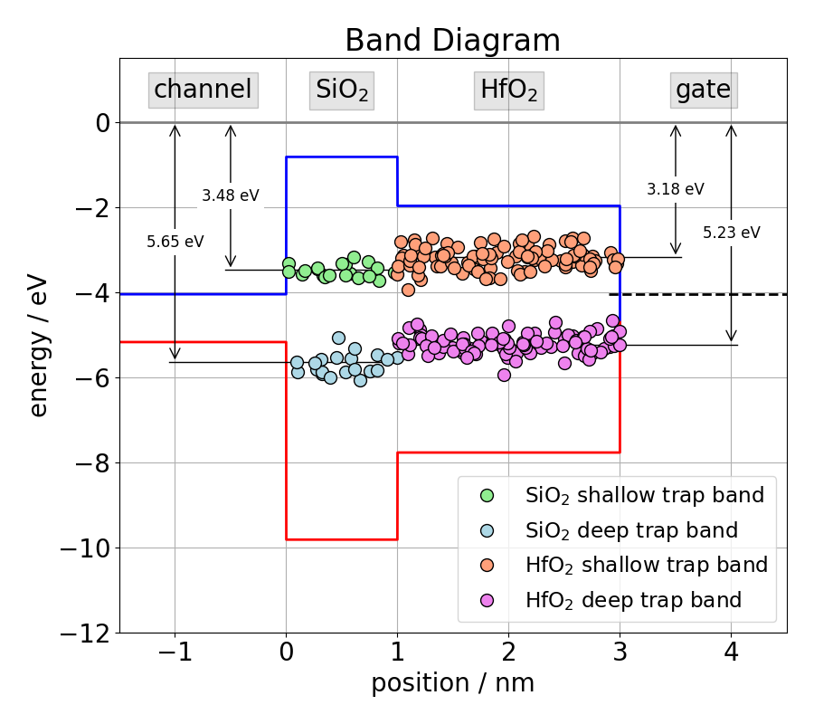
In this tutorial we will add two defect bands per oxide layer to our device: one shallow trap band whose mean energy \(\langle E_\mathrm{T} \rangle\) is closer to the conduction band edge and one deep trap band whose mean energy \(\langle E_\mathrm{T} \rangle\) is closer to the valence band edge. We assume that the shallow bands are acceptor-like and the deep bands are donor-like since this gives the smallest net charge. The mean energies of the SiO2 trap bands were chosen to be 3.48 eV and 5.65 eV and the mean energies for the HfO2 trap bands were chosen to be 3.18 eV and 5.23 eV. Fig. 2 displays these trap bands and Table 2 summarizes their properties:
comphy-band_diagram_traps
Oxide trap bands of the tutorial device. For a given defect band, the energy levels of the individual defects are normally distributed, while the spatial locations of the defects are uniformly distributed throughout the entire thickness of the respective insulator.

Parameters of the defect bands, used throughout this tutorial. In this tutorial we add one shallow acceptor-like trap band and one deep donor-like trap band per oxide laxer to the device.
defect band name x_start x_end Et Et_sigma Er Er_sigma R Nt trap_type
SiO2_shallow 0.0E-9 1.0E-9 -3.48 0.15 3.82 1.36 0.407 1.5e25 'acceptor'
SiO2_deep 0.0E-9 1.0E-9 -5.65 0.24 2.90 1.67 1.01 5.42E25 'donor'
HfO2_shallow 1.0E-9 3.0E-9 -3.18 0.16 3.19 0.77 0.59 9.05E25 'acceptor'
HfO2_deep 1.0E-9 3.0E-9 -5.23 0.15 3.55 0.741 1.01 5.16E25 'donor'
Sampling of defects In order to simulate the threshold voltage shift ΔVth caused by a band, the defects of the band have to be sampled according to the underlying distribution. This can be done by a Monte Carlo approach, i.e. by drawing random samples from the underlying distribution as displayed by the left-hand side of Fig. 3. On small devices with a limited number of defects, this approach reflects the native variability due to oxide defects and enables studies thereof. However, if the mean degradation is of interest, a large number of defects have to sampled with this approach to get an accurate result. A direct efficient way to compute the mean degradation compared to sampling a large number of defects in a Monte Carlo fashion, is to sample the defects on a grid. For this purpose, the parameter space is discretized with a certain step size, resulting in a equidistant grid as shown on the right-hand side in Fig. 3. Next, the defects are distributed on the grid points according to weights representing the underlying distribution of the defect band. In this tutorial we will stick with this approach rather than Monte Carlo sampling.
comphy-band_diagram_traps
Sampling of defects on an equidistant grid. The total number of traps is distributed on the grid points according to weights representing the underlying distribution of the defect band.

Now we are ready to add the oxide traps to our device. First we create a GaussianGridSampler, that handles the sampling of the defects as described above. The GaussianGridSampler requires the grid spacing of the parameter space as input. Each axis of the parameter space can be discretized with a different step size: grid_sampler = GaussianGridSampler(
dxt=1.0E-10, # grid spacing for sampling xt in m
dEt=0.05, # grid spacing for sampling of Et in eV
dEr=0.1, # grid spacing for sampling of Er in eV
non_coverage=1.0E-4, # sets boundary of gaussian grid
)

Now we can add defect bands one by one to our device according to Table 2: SiO2_shallow_trap_band = TrapBand_2S_NMP(
x_start=0.0E-9, # lower bound of spatial defect distribution in m
x_end=1.0E-9, # upper bound of spatial defect distribution in m
Et=-3.48, # mean energy level in eV
Et_sigma=0.15, # standard dev. of energy level in eV
Er=3.82, # mean relaxation energy in eV
Er_sigma=1.36, # standard dev. of relaxation energy in eV
R=0.407, # curvature ratio
Nt=1.5e25, # defect concentration in m⁻³
trap_type='acceptor', # type of traps
sampler=grid_sampler, # a appropriate grid sampler
device=my_device, # the device to which you want to add the traps
)

my_device.trap_bands['SiO2_shallow_trap_band'] = SiO2_shallow_trap_band

SiO2_deep_trap_band = TrapBand_2S_NMP(
x_start=0.0E-9, # lower bound of spatial defect distribution in m
x_end=1.0E-9, # upper bound of spatial defect distribution in m
Et=-5.65, # mean energy level in eV
Et_sigma=0.24, # standard dev. of energy level in eV
Er=2.90, # mean relaxation energy in eV
Er_sigma=1.67, # standard dev. of relaxation energy in eV
R=1.01, # curvature ratio
Nt=5.42E25, # defect concentration in m⁻³
trap_type='donor', # type of traps
sampler=grid_sampler, # a appropriate grid sampler
device=my_device, # the device to which you want to add the traps
)

my_device.trap_bands['SiO2_deep_trap_band'] = SiO2_deep_trap_band

HfO2_shallow_trap_band = TrapBand_2S_NMP(
x_start=1.0E-9, # lower bound of spatial defect distribution in m
x_end=3.0E-9, # upper bound of spatial defect distribution in m
Et=-3.18, # mean energy level in eV
Et_sigma=0.16, # standard dev. of energy level in eV
Er=3.19, # mean relaxation energy in eV
Er_sigma=0.77, # standard dev. of relaxation energy in eV
R=0.59, # curvature ratio
Nt=9.05E25, # defect concentration in m⁻³
trap_type='acceptor', # type of traps
sampler=grid_sampler, # a appropriate grid sampler
device=my_device, # the device to which you want to add the traps
)

my_device.trap_bands['HfO2_shallow_trap_band'] = HfO2_shallow_trap_band

HfO2_deep_trap_band = TrapBand_2S_NMP(
x_start=1.0E-9, # lower bound of spatial defect distribution in m
x_end=3.0E-9, # upper bound of spatial defect distribution in m
Et=-5.23, # mean energy level in eV
Et_sigma=0.15, # standard dev. of energy level in eV
Er=3.55, # mean relaxation energy in eV
Er_sigma=0.741, # standard dev. of relaxation energy in eV
R=1.01, # curvature ratio
Nt=5.16E25, # defect concentration in m⁻³
trap_type='donor', # type of traps
sampler=grid_sampler, # a appropriate grid sampler
device=my_device, # the device to which you want to add the traps
)

my_device.trap_bands['HfO2_deep_trap_band'] = HfO2_deep_trap_band
Step 2: Modeling the quasi-permanent BTI component There are several degradation mechanisms in MOS structures which are not covered by charging of pre-existing oxide defects as described by the 2-state NMP model:
  • Generation and annealing of oxide defects
  • Activation and passivation of dangling bonds
  • Transformation of existing oxide defects (H relocation)
  • Metastability of pre-existing oxide defects
Which of these mechanisms dominates the quasi-permanent component depends on the processes and stress conditions. To account for the quasi-permanaent component of BTI, Comphy applies a simple double-well model with a phenomenological field dependence to interface defects. This model complements the physical 2-state NMP model and describes the quasi-permanent component reasonably well with a minimal set of parameters. The physical correspondence of this model is probably the annealing of interface defects, related to hydrogen relocation and the subsequent transformation of defect sites. The DW model employed by Comphy has two charge states separated by the thermal barrier \(\epsilon_{12}\) for charging positively and \(\epsilon_{21}\) for charging neutrally as depicted in Fig. 4:
comphy-band_diagram_traps
The double-well model has two charge states separated by the thermal barriers \(\epsilon_{12}\) and \(\epsilon_{21}\), where the former depends on the electric field \(E_\mathrm{ox}\).

While the parameter \(\epsilon_{21}\) is an input quantity in Comphy, \(\epsilon_{12}\) depends on the electric field \(E_\mathrm{ox}\) at the oxide interface and the input quantities \(\gamma \) and \(\epsilon_{12,0}\) as: \begin{equation} \epsilon_{12} = \epsilon_{12,0} - \gamma E_\mathrm{ox} \end{equation} In this way, the depassivation is modeled with a field dependence whereas the passivation does not depend on the electric field. This is in line with the qualitative observation regarding the characteristics of the recoverable and the quasi-permanent BTI component. Based on these barriers, the transition rates between state 1 and state 2 are calculated in a semi-classical fashion, with the Boltzmann factor: \begin{equation} k_{12} = k_0 e^{ - \beta \epsilon_{12}} \end{equation} \begin{equation} k_{21} = k_0 e^{ - \beta \epsilon_{21}} \end{equation} where \(k_0\) denotes the transition rate for zero barrier. For a more detailed description of the employed DW model and its parameters please refer to G. Rzepa et al. "Comphy - A Compact-Physics Framework for Unified Modeling of BTI", Microelectronics Reliability, 2018.

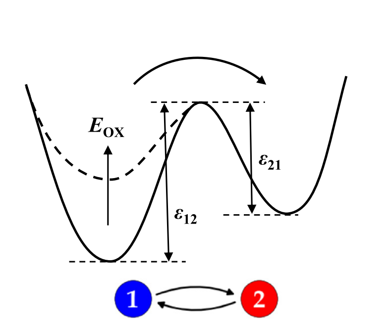
Similar to the Gaussian NMP trap band, we assume \(\epsilon_{12,0}\) and \(\epsilon_{21}\) to be normally distributed while the other parameters are approximated as constant. Consequently, a Gaussian DW defect band can be described in the Comphy framework by the following 8 parameters:

Parameters of Gaussian DW defect band
parameter Comphy notation description unit
\(\langle \epsilon_{12,0} \rangle \) eps1 mean activation energy barrier eV
\( \sigma_{\epsilon_{12,0}} \) eps1_sigma standard deviation of activation energy barriers eV
\(\langle \epsilon_{21} \rangle \) eps2 mean passivation energy barrier eV
\( \sigma_{\epsilon_{21}} \) eps2_sigma standard deviation of passivation energy barriers eV
\( k_0 \) k0 transition rate for zero barrier s⁻¹
\( \gamma \) gamma empirical field dependence of activation barrier eV m V⁻¹
\( N_\mathrm{t} \) Nt interface defect concentration m⁻²
-- trap_type type of traps (either donor or acceptor) --


In this tutorial we want to add a single donor-like interface defect band to our device using the double-well model. The parameters of the defect band that we will add to our device are summarized in Table 4:
Parameters of interface defect band, used throughout this tutorial.
defect band name eps1 / eV eps1_sigma / eV eps2 / eV eps2_sigma / eV k0 / s gamma / eV m V⁻¹ Nt / m⁻² trap_type
interface_traps 2.5297 0.92612 1.649 0.060114 1.2336E+13 1.7052E-10 1.9096E+17 donor


Now we are ready to create the double-well interface defects and add them to our device. Again, in the same way as for 2-state NMP defects, the double-well defects can be sampled with a Monte Carlo approach or on a grid. In this tutorial we will stick with the grid sampling. Consequently, in a first step we create a InterfaceGridSampler, that handles the sampling. interface_grid_sampler = InterfaceGridSampler(
d_eps1=0.1, # grid spacing for sampling eps_1 in eV
d_eps2=0.001, # grid spacing for sampling eps_2 in eV
)
Next we can create the DW interface defects according to Table 2 and add them to our device: interface_traps = GeneratedInterfaceTraps(
eps1=2.5297, # mean activation energy barrier in eV
eps1_sigma=0.92612, # standard dev. of activation energy barriers in eV
eps2=1.649, # mean passivation energy barrier in eV
eps2_sigma=0.060114, # standard dev. of passivation energy barriers in eV
k0=1.2336E13, # transition rate for zero barrier in s⁻¹
gamma=1.7052e-10, # field dependence of activation barrier in eV m V⁻¹
Nt=1.9096E17, # interface defect density
trap_type='donor', # type of traps
sampler=interface_grid_sampler, # interface grid sampler
device=my_device, # the device to which you want to add the traps
)
Step 3: Initializing the device In this section we successfully added NMP oxide defects and DW interface defects to our device. Now let's initialize the device: # initialize devices
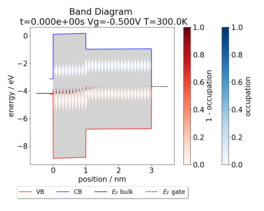
my_device.initialize(
Vg=-0.5, T=Temperature,
min_number_steps=10,
max_number_steps=100,
max_time=1.0E100,
threshold=1.0E-65,
debug=True
)

During initialization, Comphy tries to reach the equilibrium occupancy of the traps in an iterative manner, starting from an initial occupancy of 0.5. The device is considered in equilibrium once the convergence rate \( (1/V_\mathrm{th}) \cdot (dV_\mathrm{th}/dt) \) falls below the specified threshold. If no threshold is specified a default threshold of 1.0E-80 s⁻¹ is used. If debug is set to true, a summary of the equilibration process will be plotted, showing the threshold voltage and the convergence rate at each time step (see Fig. 5). In order to speed up the initialization, the convergence criterion can be relaxed by increasing the threshold or decreasing max_number of steps. Note, however, that this has the side effect that the resulting device state deviates more from true equilibrium.
comphy-init
Summary of equilibration process showing the threshold voltage shift and convergence rate of each time step.

After the initialization you can plot the equilibrium occupation of the trap bands using the plotting library that comes with Comphy: # plot band diagram
plot_band_diagram(my_device)
The above line should result in Fig. 6 showing the equilibrium occupancy of the trap bands, which obeys the Fermic-Dirac distribution. Note that for acceptor traps the occupancy is plotted to display the trapped electrons, while for donor traps one minus the occupancy is plotted to display the trapped holes.
comphy-init
This plot shows the band diagram and the occupancy of the traps after the initialization. Essentially all traps are unfilled, reflecting Fermi-Dirac statistics.