Trap-Assisted Tunneling (TAT) A unified approach for TAT and BTI While the most pronounced effects of charge trapping by oxide defects are electrostatic shifts manifesting as BTI or random telegraph noise, the same mechanism can also lead to gate leakage current by conductance over defects, which is commonly known as trap assisted tunneling (TAT).

Although several different models to describe TAT have been proposed in the literature, it is usually treated separately from charge trapping in the context of BTI. To unify the description of TAT and BTI, Comphy implements a novel approach, in which both phenomena are described on the basis of the NMP model. In contrast to previous approaches, this unified description enables the simulation of TAT and BTI with a reduced and consistent defect parameter set.

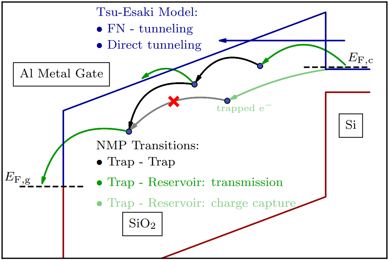
Fig. 1 shows a schematic of this new approach. The band-to-band tunneling mechanisms (blue) are modeled in Comphy using the well-known Tsu-Esaki model and the Wentzel-Kramer-Brillouin (WKB) approximation, while all trap-assisted tunneling processes (green and black) are described by two-state NMP transitions:

comphy-band_diagram_traps
The different tunneling mechanisms that typically appear in a MOS device are shown schematically. The band-to-band tunneling mechanisms are displayed in blue and the trap-assisted tunneling reactions are visualised in green.

This section was a brief summary of the publication D. Waldhoer et al. "Comphy v3.0 -- A Compact-Physics Framework for Modeling Charge Trapping Related Reliability Phenomena in MOS Devices". An in-depth description of the employed models can be found in the related publication C. Schleich et al. "Single- Versus Multi-Step Trap Assisted Tunneling Currents—Part I: Theory". In order to gain a more detailed understanding of the unifed approach for the simulation of TAT and BTI we encourage you to read both papers. Performing your own TAT simulation Once you have created your device you can add defect bands of type TrapBand_2S_NMP_3D to it, to build the foundation for the TAT simulation. Note, that in the context of TAT simulations a PseudoMC3Dsampler is required for defect sampling: pseudo_mc3d_sampler = PseudoMC3Dsampler(
N=N, # average number of defects per slab
Dens=Nt, # defect density in m⁻³
)

SiO2_TAT_trap_band = TrapBand_2S_NMP_3D(
x_start=0.0E-9, # lower bound of spatial defect distribution in m
x_end=1.0E-9, # upper bound of spatial defect distribution in m
Et=-2.37, # mean energy level in eV
Et_sigma=0.1, # standard dev. of energy level in eV
Er=0.892, # mean relaxation energy in eV
Er_sigma=0.1, # standard dev. of relaxation energy in eV
R=1.01, # curvature ratio
Nt=8.0E+24, # defect concentration in m⁻³
N=N_sam, # random sample from poisson distribution
ccs_traps=2E-19, # capture cross section of traps
trap_type='donor', # type of traps
sampler=pseudo_mc3d_sampler, # a appropriate grid sampler
device=my_device, # the device to which you want to add the traps
multi_TAT=True, # enables multi-step processes
)
my_device.trap_bands['SiO2_deep_trap_band'] = SiO2_deep_trap_band


After adding the desired trap bands to your device, you can use the method get_WKB_current to retrieve the current contribution, caused by band-to-band tunneling. As described above this method calculates the current based on the Tsu-Esaki model and the Wentzel-Kramer-Brillouin (WKB) approximation: J_WKB = my_device.get_WKB_current(Vg=1.4, T=0.1, detail=False)
Similarly, you can use the method apply_gate_voltage to retrieve the current contribution caused by trap-assisted tunneling reactions, if you set TATmode to True. This activates the interactions between defects and calculates the current contribution due to charge hopping. If multi_TAT is enabled also multi-step processes are considered in the calculation of the current contribution. Otherwise only single-step processes are considered. For many applications multi-step processes only become relevant for high defect densities and low relaxation energies. Thus, single-step TAT simulations provide efficient and accurate results for the majority of simulated technologies. # TAT mode activates trap interaction and calculates current due to charge hopping
dVth, band, J_TAT = my_device.apply_gate_voltage(
Vg=1.4,
time=0.1,
T=300.0,
TATmode=True,
multi_TAT=True
)

Using this approach, the threshold voltage shift and the two contributions to the tunneling current can be extracted based on a single set of defect parameters. For example Fig. 2 shows the results of a TAT simulation performed for a device with a SiC channel:
comphy-band_diagram_traps
The plot shows the results of a TAT simulation for a device with a SiC substrate, for 330K (blue) and 550K (red). The total tunneling current is calculated as sum of two contributions; one contribution caused by band-to-band tunneling and one contribution caused by trap-assisted tunneling.