Basic Usage Part1: Create your own device Welcome to the first part of the tutorial "Basic Usage". Let’s learn by example. Throughout this tutorial, we’ll walk you through the creation of your own 1-dimensional MOS device.

We are aiming for a p-channel MOS device with a 1 nm silicon dioxide and a 2 nm hafnium dioxide insulating layer. Finally, our device will be completed by a metal gate. The flat band structure of the device we are going to create is displayed in Fig. 1:
comphy-band_diagram
Band structure of the tutorial device. The gate stack consists of a silicon channel, a silicon dioxide layer, a hafnium dioxide layer and a metal gate.

This tutorial is not intended to give an in-depth insight into the physical models behind Comphy, but rather to give an introduction to using Comphy for your own simulations. For a detailed description of the employed physical models please read the publications related to Comphy.

Assembling the device It is good practice to build the device layer by layer starting from the semiconductor. We will therefore start with the definition of the silicon substrate, then move on to the SiO2 layer and the HfO2 layer and finally define the properties of the gate.
Step 1: Create the device object: We start with creating our one-dimensional MOS device and set its initial temperature to room temperature (~300K). Temperature = 300.0
my_device = MOS_1D(
Tinit=Temperature, # initial temperature in K
)
Now that we have created our device object, we can add the different layers of the stack. Step 2: Add semiconductor channel: To create the semiconductor channel, we need a bandgap model describing how the bandgap of the semiconductor depends on temperature. Comphy offers three predefinied bandgap models in the Physics module:
  • The first model BandGapModel_constant has a constant bandgap \(E_\mathrm{g}(T) = E_\mathrm{g0}\).
  • The second model BandGapModel_Tdep1 exhibits a linear temperature dependence \(E_\mathrm{g}(T) = E_\mathrm{g0} + E_\mathrm{g1} \cdot T \).
  • The third model BandGapModel_Tdep2 has a more complicated temperature dependence \(E_\mathrm{g}(T) = E_\mathrm{g0} + E_\mathrm{g1} \cdot T + E_\mathrm{g2} * T² / (T + E_\mathrm{dg}) \) that matches the temperature dependence used on http://www.ioffe.ru/SVA/NSM/Semicond/Si/.
Let's choose the bandgap model with the linear temperature dependence for our device and enter the respective parameters fo silicon: bandgap_model = BandGapModel_Tdep1(
Eg0=1.206, # band gap parameter in eV
Eg1=-2.73E-4, # band gap parameter in eV/K
)


Next we create the carrier models describing how the electrons and holes in the semiconductor react to temperature and bias. Again, the entered material parameters correspond to those of silicon: e_model = CarrierModel_Electrons_1(
Ncv0=2.541E25, # effective density of states of conduction band
Mc=6, # equivalent minima of conduction band
mt0=0.1905, # transversal effective mass
ml=0.9163, # longitudinal effective mass
bgmodel=bandgap_model, # bandgap model
)


h_model = CarrierModel_Holes_1(
Ncv0=2.54E25, # effective density of states of valence band
mEff_a=0.4435870, # effective mass parameter
mEff_b=0.3609528e-2, # effective mass parameter in K⁻¹
mEff_c=0.1173515e-3, # effective mass parameter in K⁻²
mEff_d=0.1263218e-5, # effective mass parameter in K⁻³
mEff_e=0.3025581e-8, # effective mass parameter in K⁻⁴
mEff_f=0.4683382e-2, # effective mass parameter in K⁻¹
mEff_g=0.2286895e-3, # effective mass parameter in K⁻²
mEff_h=0.7469271e-6, # effective mass parameter in K⁻⁶
mEff_i=0.1727481e-8, # effective mass parameter in K⁻⁸
)

Each carrier model defines the effective mass, the density of states and the concentration of the respective carrier type. Consequently, the most important methods that all carrier model classes have in common are get_m_eff(), get_DOS() and get_carrier_conc(), which can be used to retrieve the effective mass, the density of states and the carrier concentration respectively.

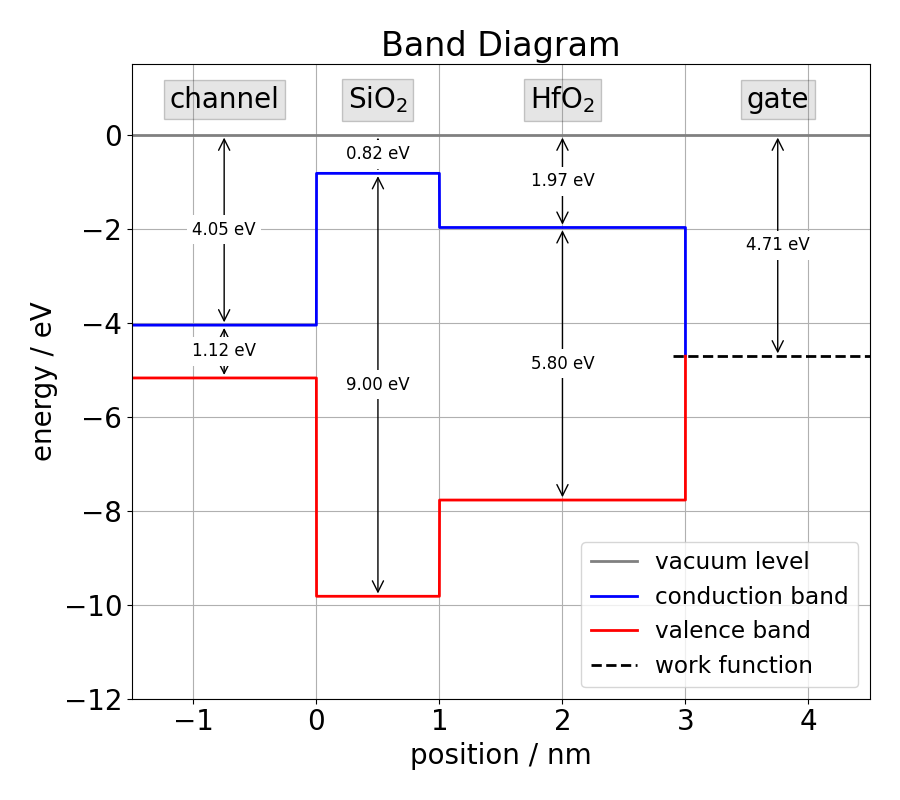
Finally, we have everything at hand to create the semiconductor substrate. In order to define the substrate, we need to pass the donor concentration Nd, the acceptor concentration Na, the relative permittivity kval, the electron affinity Xsi and the capture-cross-section ccs_e/ccs_h for electrons and holes as parameters to the constructor of the Channel class. We will create an n-type substrate with a donor concentration of 1.4E23 m⁻³ and an acceptor concentration of 1.0E16 m⁻³ for our device (Note that the concentrations are entered in SI units and not in cm⁻³). Once we have created the substrate, we can add it to the existing device.
Si = Channel(
Nd=1.4E23, # donor concentration in m⁻³
Na=1.0E16, # acceptor concentration mass in m⁻³
name='Si', # material name
Eg=bandgap_model, # band gap model of channel
m_neff=e_model, # electron effective mass (or carrier model)
m_peff=h_model, # hole effective mass (or carrier model)
Xsi=4.05, # electron affinity in eV
kval=11.68, # relative permittivity
ccs_e=2.0E-23, # capture cross section for electrons in m⁻²
ccs_h=2.0E-23, # capture cross section for holes in m⁻²
)
my_device.channel = Si
Step 3: Add oxide layers: In our next step we define the insulating layers and add them to our device. Each insulating layer requires as input parameters the layer thickness, the relative permitivity kval, the bandgap Eg, the electron affinity Xsi, the material_name and the tunneling mass mt. The bandgap can either be initialized with a simple float to define a constant bandgap, or with a corresponding temperature-dependent bandgap model as in the case of the silicon channel. To keep this tutorial as simple as possible, we assume constant band gaps for the oxide layers: SiO2 = InsulatingLayer(
thickness=1.0E-9, # thickness of layer in m
kval=3.9, # relative permittivity
Eg=9.0, # band gap in eV (or bandgap model)
Xsi=0.82, # electron affinity in eV
material_name='SiO2', # name of layer-material
mt=0.35, # relative tunneling mass
)
my_device.insulating_layers.append(SiO2)

HfO2 = InsulatingLayer(
thickness=2.0E-9, # thickness of layer in m
kval=20.0, # relative permittivity
Eg=5.8, # band gap in eV (or bandgap model)
Xsi=1.972, # electron affinity in eV
material_name='HfO2', # name of layer-material
mt=0.17, # relative tunneling mass
)
my_device.insulating_layers.append(HfO2)

Note that the order in which the layers are added to the device reflects the order of the materials in the gate stack. This means that the layer closer to the semiconductor substrate must be added first. Step 4: Add gate: Finally, to finish the stack we add a metal gate to our device. To create the gate we need to pass the workfunction of the gate material, the capture cross section ccs and a descriptive name to the constructor of the Metal class. For this tutorial, we choose TiN gate with a work function of 4.71 eV as displayed in Fig. 1: gate = Metal(
workfunction=4.71, # work function in eV
name='metalgate', # name of gate-material
ccs=2.0E-23, # capture cross section for electrons in m⁻²
)
my_device.gate = gate

Step 5: Print basic device properties: In order to get familiar with the framework, we want to retrieve and print some basic properties of our device. We want to print the flatband voltage, the threshold voltage, the equivalent oxide thickness, the doping concentrations and the Fermi level in the semiconductor. To retrieve the respective quantities from our device object we initialize the device and use the methods my_device.get_Vfb0, my_device.get_Vth0, my_device.EOT, my_device.Nd, my_device.Na and my_device.get_Fermilevel: # print basic device properties

print("Vfb0 = %.3f V" % my_device.get_Vfb0(T=Temperature))

print("Vth0 = %.3f V" % my_device.get_Vth0(T=Temperature))

print("EOT = %.3f nm" % my_device.EOT * 1.0E9)

print("Nd = %.3e cm⁻³" % my_device.channel.Nd * 1.0E-6)

print("Na = %.3e cm⁻³" % my_device.channel.Nd * 1.0E-6)

print("Ef = %.3f eV" % my_device.channel.get_Fermilevel(T=Temperature))

for i, layer in enumerate(my_device.insulating_layers):
print("layer {}:".format(i), layer)
Note that there is a difference between my_device.get_Vth0 and my_device.Vth. The method my_device.get_Vth0 always returns the threshold voltage of the ideal device. Contrary, my_device.Vth returns the threshold voltage including the effect of whatever charge is trapped in the oxide. If you followed the tutorial carefully, you should see the following output when running the Python snippet above: Vfb0 = 0.521 V
Vth0 = -0.404 V
EOT = 1.390 nm
Nd = 1.400e+17 cm⁻³
Na = 1.000e+10 cm⁻³
Ef = -4.189 eV
layer 0: 1.00nm SiO2
layer 1: 2.00nm HfO2
Step 5: Plot flatband diagram: Finally, we want to plot the flatband diagram of our device as a consistency check. For this purpose we initialize the device with the flatband voltage obtained above and use the plotting script plot_band_diagram that comes with Comphy. # initialize devices
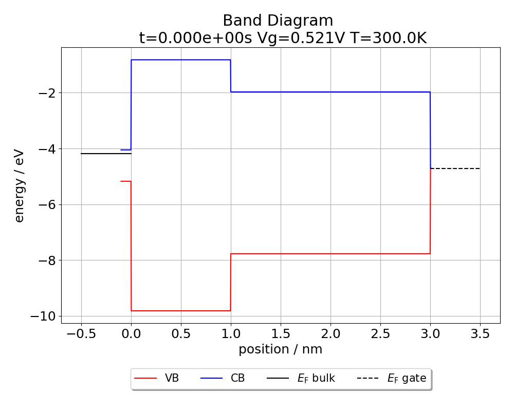
my_device.initialize(Vg=0.521, T=Temperature)

# plot band diagram
plot_band_diagram(my_device)
Note that by default the method plot_band_diagram uses the last applied gate voltage for the calculation of the device electrostatics. Since we initialized our device with the flatband voltage, executing the above Python snippet should result in the following flatband diagram:
comphy-band_diagram_traps
The figure shows the flat band diagram of our tutorial device.