Basic Usage Part3: Performing a simple BTI simulation
Welcome to the third part of the tutorial "Basic Usage".
In this part you will learn how to perform a simple BTI simulation for the device created previously.
First, you will learn how to extract basic device characteristics to get familiar with the framework. Then, we will calculate the surface potential,
the potential profile across the stack and the electric field across the stack. Finally, we will calculate the threshold voltage shift \(\Delta V_\mathrm{th} \) for a selected stress pattern. Step 1: Print basic device properties
For the beginning we want to print some basic properties of our device, to get familiar with the framework.
We want to print the flatband voltage and the threshold voltage after the initialization and compare it with the
flatband voltage and threshold voltage of the ideal device:
# print basic device properties
print("Vth = {:.3f} V".format(my_device.Vth))
The above Python snippet should result into follwing output.
Vfb0 = 0.521 V
Vth0 = -0.404 V
Vfb = 0.518 V
Vth = -0.407 V
We find that right after initialization there is a voltage shift of 40mV between the ideal device and the device with charges in the oxide.
Everything seems fine so far and we can continue with our simulation.
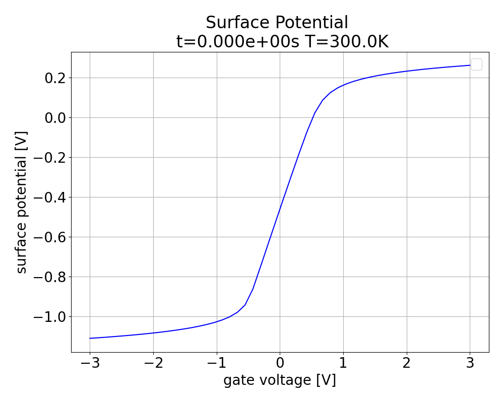
Step 2: Plot surface potential
Now that we checked our device we want to plot the surface potential,
i.e. the potential difference between the surface and the bulk of the semiconductor.
Since most TCAD tools are capable of calculating the semiconductor potential, it is a good metric to compare other TCAD tools with Comphy.
To plot the surface potential we use the method plot_semiconductor_potential provided by the plotting library of Comphy.
Note that the calculation of the surface potential assumes all charges currently present in the oxide to be stationary.
# plot semiconductor potential
plot_surface_potential(my_device)
The above Python snippet should produce the following image:
The plot shows the surface potential, i.e. the potential difference between the surface and the bulk of the semiconductor, of our tutorial device.
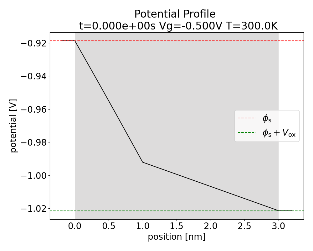
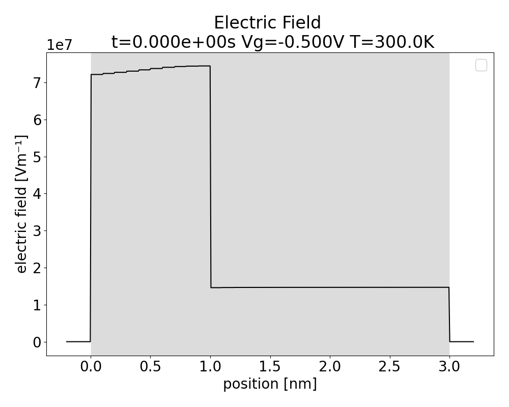
Step 3: Calculate potential profile and electric field across the stack
In our next step we want to plot the potential profile and the electric field across the stack for the equilibrium.
For this purpose we use the methods plot_potential_profile and plot_electric_field from the plotting library:
plot_potential_profile(my_device)
plot_electric_field(my_device)
The above Python snippet should result in Fig. 2. and Fig. 3. Note that Comphy uses a surface-potential-based compact model and hence does not calculate the full potential profile in the semiconductor.
The method plot_potential_profile(my_device) plots the potential at the semiconductor surface instead of the actual potential for x-values smaller than zero!
Nevertheless, Comphy is able to display the correct potential and electric field in the insulating layers, which displays the effect of the oxide charges.
Due to the oxide charges, the electric field in the oxide layers is no longer constant (see Fig. 3).
Note that the finer the spatial resolution of the gridsampler is chosen, the smoother the curves will be.
The plot shows the potential profile across the stack for our tutorial device.
Note that the constant potential profile in the semiconductor does not correspond to reality, but arises from the limitations of the compact model.
The plot shows the electric field across the stack for our tutorial device.
Note that the vanishing electric field in the semiconductor does not correspond to reality, but arises from the limitations of the compact model.
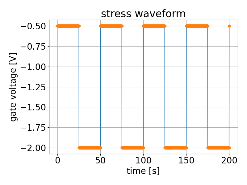
Step 4: Define stress pattern
Finally, we want to deflect the device out of equilibrium, by applying a stress pattern.
For this purpose we start with the definition of the stress pattern.
For demonstration we want to stress our device with a square signal with a frequency of (1.0 / 50.0) s⁻¹ for a total time of 200 seconds.
During the application of the stress we will keep the device at a constant temperature of 300.0 K.
# define stress pattern
# define time steps
time_per_step = 0.1
number_steps = 2000
time = np.linspace(0.0, time_per_step * number_steps, number_steps)
# define constant temperature profile
temperature = np.full_like(time, 300.0)
# define gate voltage profile
min = -2.0
max = -0.5
frequency = 1.0 / 50.0
Vg = min + (max - min)*(signal.square(2 * np.pi * frequency * time)/2.0 + 0.5)
# plot gate voltage profile
figure = plt.figure(figsize=(8.0, 6.0))
plt.plot(time, Vg)
plt.plot(time, Vg, 'o')
plt.title("stress waveform")
plt.xlabel("time / s")
plt.ylabel("gate_voltage / V")
plt.tight_layout()
plt.grid()
plt.show()
The plot shows the stress waveform for the BTI simulation
Step 5: Calculate shift of threshold voltage
Now we are ready to apply the stress pattern to our device.
In the following we want to store the threshold voltage of the equilibrated device as reference.
Then we apply the stress to our device and store the threshold voltage shift with respect to the reference for plotting.
# apply stress pattern to device
# let's initialize the device with the initial voltage and temperature
my_device.initialize(Vg=Vg[0], T=temperature[0])
# Now, let's retrieve the threshold voltage of the unstressed device as reference
Vth_ref = my_device.Vth
# Now, we create a list to collect the threshold voltage shifts
threshold_voltage_shifts = [0.0]
# Now, we loop over the scenario we have set out. # We skip the first point as that is our initialization point. for idx inrange(1, len(time)):
# here we actually apply the voltage for a given timestep
my_device.apply_gate_voltage(
Vg=Vg[idx], T=temperature[idx], dt=time[idx] - time[idx-1],
) # now let's retrieve the threshold voltage after application of stress
new_Vth = my_device.Vth
# finally, we store the threshold voltage shift w.r.t the reference point
threshold_voltage_shifts.append(new_Vth - Vth_ref)
# Now that we have the data, let's plot it
figure = plt.figure(figsize=(8.0, 6.0))
plt.plot(time, np.abs(threshold_voltage_shifts))
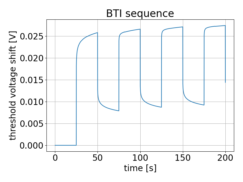
plt.title("BTI sequence")
plt.xlabel("time / s")
plt.ylabel("dVth / V")
plt.tight_layout()
plt.grid()
plt.show()
The above Python snippet yields the following image:
The plot shows the shift of the threshold voltage of our device when stressed with the waveform displayed in Figure 4.0
Congratulations, you performed your first BTI simulation and calculated the threshold voltage shift \(\Delta V_\mathrm{th} \) with the Comphy framework.
In the same way, you can calculate the threshold voltage shift for arbitrary stress profiles. At this point we recommend playing with the parameters of the trap bands to get a feeling for the effect of each parameter.